Introduction
In today's technologically advanced world, the Printed Wiring Board (PWB) has become an indispensable component in countless electronic devices. Whether it's your smartphone, laptop, or home appliances, PWBs are at the heart of these gadgets, enabling seamless communication and functionality. This article will take you on a captivating journey through the evolution of PWBs, exploring their manufacturing process, different types, and the numerous benefits they bring to various industries.
The Fascinating World of Printed Wiring Boards
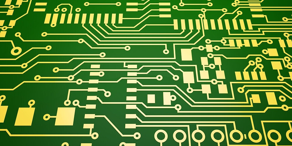
Printed Wiring Boards, commonly known as circuit boards or PCBs, are intricate platforms that serve as a foundation for electronic components to connect, communicate, and function harmoniously. These boards play a vital role in the world of electronics, enabling the seamless flow of information and power within devices of all shapes and sizes.

PRINTED WIRING BOARD - A Technological Breakthrough
The concept of the Printed Wiring Board revolutionized the electronics industry when it was first introduced. Prior to its advent, electronic components were connected through a time-consuming and error-prone manual wiring process. The introduction of PWBs automated the manufacturing process, making it more efficient, cost-effective, and reliable.
Subheading: The Birth of PWB
The origins of the Printed Wiring Board can be traced back to the mid-20th century. The need for more efficient wiring methods arose as the complexity and miniaturization of electronic devices increased. This led to the development of a revolutionary technique that involved etching copper pathways onto an insulating substrate, giving birth to the modern Printed Wiring Board.
PRINTED WIRING BOARD - Unveiling the Manufacturing Process
The manufacturing process of Printed Wiring Boards is a meticulous and intricate procedure that involves several key steps. Let's delve into the journey of a PWB from conception to completion.
Subheading: Step 1 - Design and Schematic Capture
The first step in manufacturing a PWB involves designing the circuit and capturing the schematic. Designers utilize specialized software to create the layout and plan the electrical connections between components.
Subheading: Step 2 - Substrate Selection
Once the design is finalized, the next crucial step is selecting the appropriate substrate material. The choice of substrate depends on factors such as heat resistance, flexibility, and desired electrical properties.
Subheading: Step 3 - Applying Copper Layer
In this step, a thin layer of copper is laminated onto the substrate material. The copper layer will serve as the conductive pathways for electrical signals to flow.
Subheading: Step 4 - Etching and Tracing
To create the circuitry pattern, a photoresist is applied to the copper layer, and the unwanted copper is etched away using a chemical process. The remaining copper traces form the intricate pathways required for the functioning of the electronic components.
Subheading: Step 5 - Drilling and Plating
After the etching process, holes are drilled into the board to accommodate component leads and vias. These holes are then plated with a conductive material to establish electrical connections between different layers of the PWB.
Subheading: Step 6 - Component Assembly
Once the board is ready, electronic components such as resistors, capacitors, and integrated circuits are mounted onto the PWB. This process is typically automated to ensure precision and efficiency.
Subheading: Step 7 - Soldering
The final step involves soldering the components onto the board, creating a secure and reliable connection. Advanced soldering techniques, such as surface mount technology (SMT) or through-hole technology (THT), are employed depending on the specific requirements of the PWB.

Types of Printed Wiring Boards
Printed Wiring Boards come in various types, each designed to cater to specific needs and applications. Let's explore some common types of PWBs:
Subheading: Single-Sided PWBs
Single-sided PWBs consist of a single layer of conductive material, usually copper, on one side of the substrate. These boards are commonly used in simpler electronic devices and applications with lower circuit complexity.
Subheading: Double-Sided PWBs
Double-sided PWBs feature conductive material on both sides of the substrate. This allows for more complex circuitry and increased component density. Double-sided PWBs are widely used in a range of applications, including consumer electronics, automotive systems, and medical devices.
Subheading: Multilayer PWBs
Multilayer PWBs are composed of multiple layers of conductive material separated by insulating layers, called substrates. These boards offer higher circuit density and are capable of accommodating complex designs with multiple interconnected layers. Multilayer PWBs are commonly used in high-performance electronic devices such as smartphones, computers, and aerospace systems.
Subheading: Flexible PWBs
As the name suggests, flexible PWBs are designed to be flexible and bendable. They are made using flexible substrate materials such as polyimide or polyester. Flexible PWBs are ideal for applications that require adaptability and space-saving, such as wearable devices, medical sensors, and automotive electronics.
Subheading: Rigid-Flex PWBs
Rigid-flex PWBs combine the best of both worlds by incorporating both rigid and flexible sections within a single board. This allows for seamless integration of components and circuits in complex geometries. Rigid-flex PWBs are widely used in aerospace, military, and medical applications where reliability and space optimization are critical.
Benefits of Printed Wiring Boards
Printed Wiring Boards offer a plethora of benefits that make them the preferred choice in electronic design and manufacturing. Let's explore some key advantages of using PWBs:
Subheading: Compactness and Space Optimization
PWBs allow for the integration of complex circuitry and components within a compact form factor. This enables the creation of smaller and lighter electronic devices, making them more portable and space-efficient.
Subheading: Improved Reliability
The automated manufacturing process of PWBs ensures precision and consistency, minimizing the risk of human error. Additionally, the use of advanced materials and techniques enhances the reliability and longevity of electronic devices.
Subheading: Enhanced Electrical Performance
Printed Wiring Boards offer excellent electrical properties, including low signal loss, controlled impedance, and reduced electromagnetic interference. These characteristics result in improved signal integrity and overall performance of electronic systems.
Subheading: Cost Efficiency
The mass production capabilities of PWBs make them a cost-effective solution for electronic manufacturing. The automation and efficiency in the manufacturing process translate into reduced labor costs and increased economies of scale.
Subheading: Design Flexibility
PWBs provide designers with the freedom to create complex circuit layouts and incorporate innovative designs. The use of multilayer boards, flexible materials, and advanced manufacturing techniques allows for versatile and creative electronic designs.
Subheading: Time-to-Market Advantage
The streamlined manufacturing process of PWBs reduces the time required for production and assembly. This enables faster product development cycles, allowing companies to bring their electronic devices to market more quickly, gaining a competitive edge in the industry.
Frequently Asked Questions about Printed Wiring Boards
Here are some frequently asked questions about Printed Wiring Boards along with their answers:
FAQ 1: What is the role of Printed Wiring Boards in electronic devices?
Printed Wiring Boards serve as a platform for connecting and supporting electronic components, allowing them to function together and communicate seamlessly.
FAQ 2: Are all Printed Wiring Boards the same size?
No, Printed Wiring Boards come in various sizes, depending on the specific application and device requirements. They can range from small, compact boards used in wearable devices to larger boards used in industrial equipment.
FAQ 3: Can Printed Wiring Boards be repaired if they malfunction?
In some cases, yes. If a specific component or trace on the board is identified as faulty, it can be replaced or repaired. However, extensive damage or issues with the board's core structure may necessitate the replacement of the entire board.
FAQ 4: Are Printed Wiring Boards environmentally friendly?
Printed Wiring Boards have made significant advancements in terms of environmental friendliness. Manufacturers strive to use materials that are compliant with regulations and industry standards to minimize the environmental impact. Recycling initiatives for electronic waste, including Printed Wiring Boards, are also being implemented.
FAQ 5: Can Printed Wiring Boards be customized for specific applications?
Absolutely. Printed Wiring Boards offer flexibility in terms of design and customization. They can be tailored to meet the specific needs of different applications, including specialized shapes, sizes, and materials.
FAQ 6: What are some emerging trends in Printed Wiring Board technology?
Some emerging trends in Printed Wiring Board technology include the development of flexible and stretchable boards for wearable electronics, advancements in miniaturization and high-density interconnects, and the integration of advanced materials for improved performance and reliability.
Conclusion
The evolution of Printed Wiring Boards has revolutionized the electronics industry, enabling the creation of sophisticated devices we rely on every day. From their humble beginnings to the advanced manufacturing processes of today, PWBs continue to play a vital role in the design, production, and functionality of electronic devices across various industries.
The compactness, reliability, cost-efficiency, and design flexibility offered by PWBs make them a crucial component in electronic systems. As technology continues to advance, we can expect further innovations in Printed Wiring Board technology, pushing the boundaries of what's possible in the world of electronics.
So, the next time you hold a sleek smartphone, marvel at a high-performance computer, or rely on the precision of medical equipment, remember that it's the Printed Wiring Board that serves as the foundation for these technological marvels.

No comments yet