
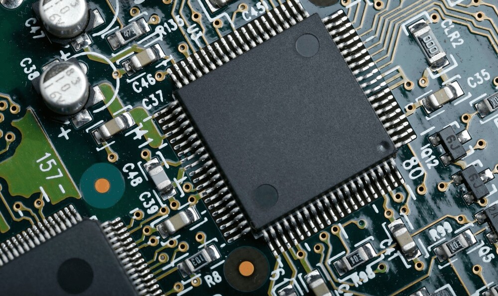
As technology advances, the need for custom PCBs becomes more apparent. Different applications require different components and circuitry, making it necessary to have a personalized PCB design.
Regarding electronic design, you must follow certain design rules to ensure a successful outcome. When it comes to PCB design, these rules are known as PCB design rules. With the help of advanced software and skilled engineers, you can design custom PCBs to meet the specific needs of a project or application.
For example, in RF device design, you must consider regulatory compliance and transmission power limitations. Additionally, power consumption is crucial for all types of miniature devices. We can create more effective and efficient devices by keeping these specific design considerations in mind.

Electrical Design Rules
Electrical design rules refer to guidelines and best practices for designing circuits or electronic systems. These rules ensure safety, functionality, and compatibility with industry standards. Some important considerations in electrical design include :
- Power Handling
- Signal Integrity
- Component Placement
- Thermal Management
By following these design rules, engineers can create efficient and reliable circuits.
Physical Design Rules
Physical design rules determine the placement and routing of components on a circuit board. These rules ensure the circuit functions properly and meet signal timing and power consumption specifications.
Some common considerations in physical design include :
- Component Spacing
- Trace Widths
- Signal Routing Priorities
These factors all affect the performance and reliability of the circuit. Additionally, physical design rules may also consider safety concerns, such as spacing between high-voltage components and accessible parts of the circuit board.
Spacing Design Rules
One of the most important considerations in PCB design service is spacing. It refers to the distance between traces, components, and other features on the board.
The primary reason for proper spacing is to prevent electrical issues such as signal interference and short circuits. Traces that are too close together can cause interference, affecting signal integrity and potentially causing errors. Similarly, components placed too close together can result in a short circuit.
Rules to Remember
There are a few common spacing rules to remember during the PCB manufacturing process.
- The trace width should be at least twice the spacing between traces, and the spacing between traces and pads should also be at least twice the trace width.
- Additionally, it is recommended to have a spacing of at least twice the component lead diameter between component leads.
PCB Layout Rules
Regarding PCB layout, you must keep the following things in mind to ensure your design turns out as expected.
1. Trace Width
The metal line's width will carry your signal, so it needs to be wide enough to handle the current flowing through it. Too narrow of a trace will lead to high resistance and signal loss, while too wide of a trace will generate excess heat.
2. Spacing between Traces
It is important because you don't want your traces to short out against each other, and second, you need to leave enough room for the traces to expand and contract with temperature changes.
3. Dielectric Constant
It will determine how well signals propagate through the board, and as such, you want to use a low dielectric constant material to minimize losses.
PCB Design Challenges
Designing a PCB is a complex task that requires knowledge of many different design rules and specifications and comes with the following challenges.
1. Size
As electronic products have become smaller and more compact, the demand for printed circuit boards (PCBs) that are smaller and thinner has also increased. It has created a challenge for PCB designers, who must now adhere to stricter design rules to create successful prototypes.
2. Multilayer PCB
One common challenge when designing a PCB is ensuring that all the different board layers are properly aligned. It can be tricky, as each layer has specific requirements and tolerances.
RF transmission PCBs
3. EMC/EMI
As electronic products become smaller and more complex, the challenge of designing printed circuit boards (PCBs) that meet electromagnetic compatibility (EMC) and electromagnetic interference (EMI) regulations becomes greater. To ensure that a PCB meets EMC/EMI standards, designers must adhere to design rules that govern the placement and routing of components and traces on the board.
4. High-frequency PCBs
Designing high-frequency printed circuit boards (PCBs) is challenging due to the need to consider many different design rules. The most important rule is ensuring that the trace widths match the transmission line impedance. It ensures no signal reflection and that the signal arrives at its destination with the correct amplitude and phase.
Software Tools Help PCB Design
The Printed Circuit Board (PCB) is the backbone of any electronic device. Software tools can help simplify the design process and produce high-quality results.
● Altium Designer
Altium Designer provides users with a complete set of tools for designing and manufacturing high-quality PCBs. It includes everything from schematic capture and PCB layout to routing and manufacturing.
● Cadence Allegro
Cadence Allegro is a powerful PCB design software tool that offers many features. One of the main features of Cadence Allegro is its ability to support multiple layers. It makes it ideal for designing complex PCBs. It also offers a wide range of other features, such as auto-routing, which can save time when designing PCBs.
● OrCAD
OrCAD is a powerful PCB design tool that helps users create high-quality designs quickly and efficiently. It provides users with tools for designing PCBs, from schematic capture and circuit simulation to board layout and routing.
● Kicad
Kicad is a great tool for both beginners and experienced PCB designers alike. It is easy to use and has a wide range of capabilities. Whether you need to design a simple circuit board or a complex multi-layer board,
● Eagle
It is PCB design software that provides users with a wide range of features and capabilities. Eagle is a popular choice for many PCB designers, as it offers a wide range of templates, libraries, and tools that You can use to create complex designs.
Conclusion
When it comes to PCB design, there are several factors to consider to ensure that your board is properly laid out. With so many different elements to consider, it's important to partner with a reliable engineering services provider who can help you with every step.
Author: Sherry Mosleh IoT Development Engineer at Arshon Technology Inc.

No comments yet