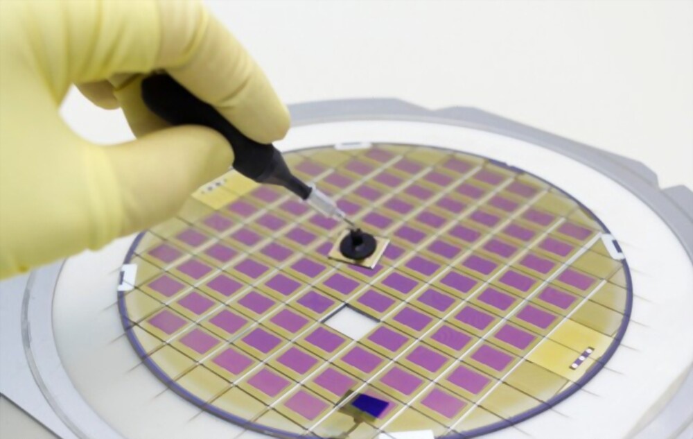
In recent years, the semiconductor industry has witnessed significant advancements in technology, leading to more efficient and sustainable manufacturing processes. One such breakthrough is the adoption of plasma dicing in semiconductor manufacturing. This technology, also known as dry etching or plasma etching, has emerged as an alternative to traditional dicing methods that involve the use of saws or lasers. This revolutionary technique offers several environmental benefits, making it an attractive choice for semiconductor manufacturers aiming to reduce their ecological footprint. This article delves into the environmental advantages of adopting this technology and its impact on sustainable semiconductor manufacturing.
How does the adoption of plasma dicing contribute to environmental benefits?
- Reduced Material Waste
This modern dicing technique significantly reduces material waste in semiconductor manufacturing. Unlike traditional methods that require a kerf (cutting width) for saw blades or lasers, the technology creates a narrow and precise cutting path. As a result, the amount of wasted material is substantially reduced, leading to better material utilization and cost savings. Additionally, the ability to perform dicing without any physical contact eliminates the risk of material breakage or damage, further minimizing waste during the manufacturing process.
- Energy Efficiency
Compared to conventional dicing techniques, this modern technique offers improved energy efficiency. Traditional methods often involve high-power lasers or mechanical saws, consuming substantial amounts of energy during the dicing process. In contrast, this advanced method utilizes plasma discharges to etch and cut the semiconductor wafers. The plasma discharge requires significantly less energy, resulting in reduced power consumption and lower environmental impact. By adopting this technology, semiconductor manufacturers can contribute to energy conservation and sustainability.
- Lower Water Consumption
This modern technology also contributes to lower water consumption in semiconductor manufacturing. Traditional dicing methods often require water-based cooling systems to prevent overheating and damage to the saw blades or lasers. These cooling systems consume large volumes of water, contributing to water scarcity and environmental strain. In contrast, the advanced dicing technique eliminates the need for water-based cooling, reducing water consumption and preserving this vital resource.
- Decreased Chemical Usage
Another environmental benefit is the decreased usage of chemicals. Traditional dicing methods may involve the application of chemical agents to facilitate the cutting process or enhance the precision of lasers. These chemicals can be hazardous and require careful handling and disposal to avoid environmental contamination. This modern dicing method, on the other hand, relies on plasma discharges and does not require the use of additional chemicals. This reduction in chemical usage minimizes the environmental impact and ensures safer manufacturing practices.
- Minimized Pollution and Emissions
The advanced technique contributes to minimizing pollution and emissions in semiconductor manufacturing. Traditional dicing methods, such as sawing or laser cutting, can generate particulate matter, smoke, and fumes that contribute to air pollution. In contrast, the modern dicing technique produces minimal particulate matter and emissions, resulting in cleaner manufacturing processes. This reduction in pollution and emissions improves the air quality within manufacturing facilities, creating a healthier working environment for employees and reducing the overall ecological impact.
What are some major eco-friendly benefits of plasma dicing?
- Improved Yield and Productivity
By adopting this modern dicing technique, semiconductor manufacturers can achieve improved yield and productivity. This advanced technique offers higher precision and accuracy compared to traditional methods, minimizing defects and enhancing the overall quality of the diced semiconductor wafers. With reduced material waste and improved yield, manufacturers can optimize their production processes, increase productivity, and meet market demands more effectively.
- Enhanced Worker Safety
This technology prioritizes worker safety in semiconductor manufacturing. Traditional dicing methods involving saws or lasers pose risks of physical injury or accidents. In contrast, the modern dicing technique eliminates the need for physical contact with the wafer, ensuring a safer working environment for employees. The absence of spinning blades or high-power lasers reduces the potential hazards and enhances worker safety, further promoting sustainable and responsible manufacturing practices.
- Cost Savings
Incorporating plasma dicing technology can lead to significant cost savings for semiconductor manufacturers. The reduced material waste, improved yield, and enhanced productivity contribute to overall cost optimization. Moreover, the energy-efficient nature of this technology results in reduced power consumption, leading to lower electricity bills. Through waste reduction and enhanced efficiency, manufacturers can achieve substantial cost savings and allocate resources more effectively.
- Scalability and Adaptability
The technology offers scalability and adaptability in semiconductor manufacturing. It can be applied to a wide range of wafer sizes, thicknesses, and materials, providing flexibility for manufacturers. Whether producing small-scale integrated circuits or large-scale semiconductor devices, this technology can accommodate diverse manufacturing requirements. This scalability and adaptability make it a versatile and future-proof solution for the semiconductor industry.
- Future Potential
The future potential of this modern technique in semiconductor manufacturing is vast. As technology continues to advance, these modern dicing techniques are likely to evolve further, offering even more efficient and sustainable solutions. The ongoing research and development in this field aim to enhance precision, increase throughput, and reduce manufacturing costs. With continuous innovation, this technology has the potential to revolutionize the semiconductor industry, paving the way for greener and more eco-friendly manufacturing practices.
Final Words
Plasma dicing has emerged as an environmentally friendly alternative in semiconductor manufacturing. Its numerous benefits, including reduced material waste, energy efficiency, lower water consumption, decreased chemical usage, minimized pollution and emissions, improved yield and productivity, enhanced worker safety, and cost savings, make it an attractive choice for manufacturers. Furthermore, this technology offers scalability and adaptability, ensuring its relevance in various semiconductor manufacturing applications. As the industry continues to evolve, this advanced dicing technique holds the potential to revolutionize semiconductor manufacturing, paving the way for a greener and more sustainable future.

No comments yet