Compact and efficient PCBs have transformed electronics production. They have facilitated the elimination of tedious hand-wiring by electronic makers, leading to greater automation of circuit manufacturing. SMT PCB stencils and high-tech placement tools have become standard equipment for modern PCB producers. Depending on the mini SMT stencil cost, various types of SMT stencils are utilized during PCB construction.
Stencil Technology
Thin layers of stainless steel or nickel are cut to specified standards by fabricators. Stencils consisting of polyester mesh and stencil foil are commonly used for low-accuracy boards because of the high cost of the process. Polyester mesh is held taut by a tensioning aluminum frame and stencil foil.
In order to classify stencils manufactured from stainless steel or nickel, it is useful to look at how the apertures or openings were formed. Both additive and subtractive procedures can be used by stencil producers.
The most frequent methods are:
- Electroforming
It's an additive method wherein the stencil is electroformed in nickel layers. Electroformed nickel stencils allow for finer pitch and smaller aperture formation. The flawless, mirror-like aperture provides an overarching framework solder paste to discharge without adhering.
During electroforming, nickel is shaped around a photo-resist template with openings that correspond to the circuit board's layout. Long processing times and high manufacturing costs at the outset are to be expected. However, the price of the stencil stays the same no matter how many holes it has cut out.
- Chemical Etching
To create an aperture, chemical etching is used, which is a subtractive technique. Etching creates rough aperture sidewalls, so while it's a cheap procedure, the results aren't great.
In chemical etching, metal sheets are pierced with acid to produce openings. Typically, production times are quick and costs are minimal. However, this technique is only useful for making big holes in the ground, and it often leaves behind a sand clock-shaped imprint on the walls. Stencils with small apertures cannot be formed using chemical etching.
- Laser Cutting
In this method, a laser beam eliminates excess material from a stencil foil (often stainless steel) to create an opening. Stencils can be made with more quality and accuracy using laser cutting. In contrast to the two approaches, laser cutting provides trapezoidal instead of vertical apertures, improving solder paste release.
Apertures with extremely fine pitch can be made with laser cutting at reasonable prices thanks to the increased accuracy of the technique. The only major drawback is the slow production speed.
Framed and Frameless Stencils
- Framed SMT stencils
They're largely usable. The mesh and the stencil are attached to an aluminum frame by the manufacturer, who attaches the mesh on one side of the stencil. The tension of the stencil is supplied by the mesh. The width and shape of a frame might change significantly depending on the printer model.
Framed SMT stencils have a larger initial investment because the operator doesn't need to buy any more accessories to get started. The operator merely needs to place it in the printer, and it will start printing. Stencils, especially the metal backing, can be reused and recycled.
- Frameless SMT stencils
You simply need to store them without frames if you want to. The thin foil stencil must be inserted by hand into a reusable frame before it can be used. Because of this, the operator can utilize various stencils inside a single frame. When production volumes are modest and the operator needs to switch to a different PCB in a hurry, frameless stencils are a viable choice.
Using SMT Stencils
- Manual Operation
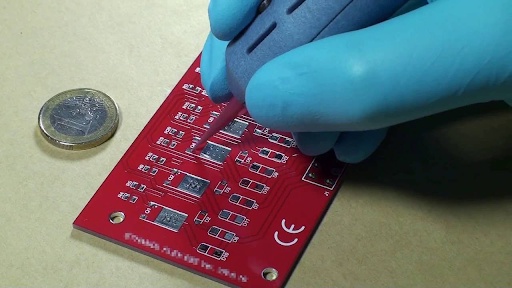
When making fewer than a few hundred boards, the operator can place each one on a tabletop. The board is held in place by two L-shaped metal plates placed on two of its opposing corners.
Aligning the stencil's fiducial markers with the PCB's own, the operator then positions the stencil and its framing on the PCB. The operator secures the stencil's frame to the table after properly aligning it with the PCB.
The stencil may be lifted off its hinged frame and the PCB can be swapped out without affecting the registration. There is a tiny space between the PCB and the stencil when the stencil is sitting flat on the board. A new printed circuit board is placed under the stencil, and the operator then applies solder paste to the stencil's top edge using a squeegee.
- Automated SMT Stencil Printing
Automated SMT stencil printers are used by PCB assemblers for high-volume production. In order to move PCBs to and from the printer, a conveyor system is integrated into the design.
Optical detectors secure a printed circuit board as it is fed into the machine. The stencil is then lowered onto the PCB, and optical sensors compare the fiducial marks on the two surfaces.
The proper amount of solder paste is subsequently dispensed from the dispenser onto the PCB, and an automated squeegee or runner carries the paste across the stencil. The stencil is removed from the board and any excess solder paste is cleaned from the underside of the stencil by the machine. A PCB is removed from the machine and a new blank board is fed in on a conveyor.

No comments yet