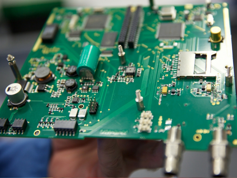
Printed circuit boards (PCBs) are essential parts in digital systems. They are small and also reliable. There are a number of different ways to design and manufacture a PCB. Although each style may have its very own subtleties, the standard steps of PCB assembly are similar. The very first step entails creating the board Then, the physical manufacturing process starts, which will likely entail laser cutting or CNC machining. After the PCB is put together, it must undergo optical assessment to make sure that the parts fit appropriately.
Printed https://pcba123.com/pcb-assembly/ setting up needs a variety of producing capabilities, as well as innovative assessment processes. One typical kind of assembly is through-hole innovation, which makes use of predrilled holes in a PCB to put electronic devices. This method guarantees that the leads are straightened properly. Though there are some makers that still by hand line up leads on elements, the bulk count on automated insertion installing devices.
It requires soldering parts to a circuit card.
As electronic products remain to grow in complexity, PCB boards are ending up being significantly little. As such, there is no solitary type of element that can be consisted of on a PCB; rather, most boards are comprised of both SMD as well as thru-hole elements. Because soldering entails numerous elements, soldering a PCB can be a complicated process.
The PCB is a critical part of any type of electronic gadget. Without it, an item will not function effectively. The process of soldering elements onto a PCB is called PCB setting up. It includes a variety of processes as well as various techniques, varying from developing a circuit card layout to soldering parts to it.
It calls for heat as well as wash
Soldering paste is an important part of the PCB assembly procedure. It is made use of to stick the individual components to the board. When it is not cleaned appropriately, it leaves residues externally of the board. These residues can be sticky as well as cause troubles with solder joints gradually. They can likewise leave a dull appearance on the final product. Dirty PCBs can be a turn off for consumers.
It requires X-ray evaluation
PCB assembly is a complicated procedure and X-ray examination is important to make certain the top quality of the ended up item. These photos can identify any kind of concealed defects beneath the surface area of the board. X-ray scanning inspection is an extremely accurate, high-throughput way to find problems. It is specifically crucial for PCBs with high-density elements and also several layers.
X-ray examination is a non-destructive means to inspect circuit boards, reducing rework as well as enhancing product quality. X-rays can penetrating multiple layers of PCBs and also can disclose concerns with wiring and solder joints. X-ray evaluation is likewise valuable in discovering hidden issues, such as short circuits and also misaligned components.
It involves part requirements
A simple PCB assembly overview includes element needs and also schematic prints. The schematic print explains the connections between board components and also suggests the required test factors. While board testers might have the ability to locate these factors on the physical PCB, they will certainly often refer to the schematic print for additional information. An example schematic is revealed listed below. The schematic additionally includes cautionary markings, which are needed to make certain the security of the set up PCB. For example, electrostatic discharge markings should exist aboard that are sensitive to static electrical energy.

No comments yet