Introduction:
Choosing the ideal PCB design india is crucial for the successful development and functionality of electronic devices. With numerous options available, finding the right PCB design can be a daunting task. This comprehensive guide aims to provide you with essential insights and factors to consider when selecting a PCB design that perfectly matches your project requirements. Whether you are a seasoned professional or a beginner, this guide will assist you in making informed decisions for your PCB design needs.
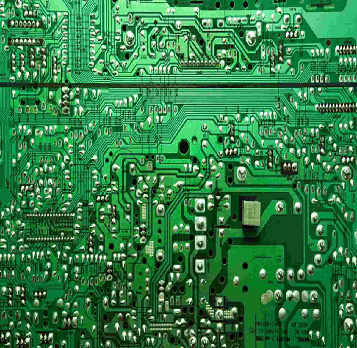
Understanding PCB Basics:
An overview of PCB (Printed Circuit Board) and its significance in electronic devices.
Explanation of the different layers, components, and materials used in PCB designs.
Introduction to the various types of PCBs, such as single-sided, double-sided, and multi-layer PCBs.
Identifying Project Requirements:
Assessing the specific requirements of your project, including size constraints, functionality, and performance expectations.
Determining the environmental factors that might affect the PCB design, such as temperature, humidity, and vibration.
Component Placement and Routing:
Guidelines for efficient component placement to optimize signal integrity, thermal management, and ease of assembly.
Techniques for routing traces and managing signal integrity, such as differential pairs and impedance control.
Factors to consider when selecting the number of layers required for your PCB design.
PCB Design Software and Tools:
Overview of popular PCB design software options and their features.
Introduction to simulation and analysis tools for verifying the integrity and performance of your PCB design.
Guidelines for selecting the appropriate tools based on your project requirements and budget.
Read Also: Advancements in PCB Manufacturing Technology in India
Design for Manufacturing (DFM) and Design for Testability (DFT):
Understanding the importance of DFM principles to ensure manufacturability and cost-effectiveness of your PCB design.
Implementing DFT strategies to facilitate the testing and debugging process during production.
Considering Manufacturing Constraints:
Addressing manufacturing constraints, such as panelization, solder mask, and copper weight.
Collaboration with manufacturers to ensure proper manufacturability and cost optimization.
Quality Assurance and Testing:
Overview of quality control processes to ensure the reliability and functionality of the manufactured PCBs.
Techniques for testing and inspecting PCBs, including automated testing and visual inspection methods.
Importance of reliability testing, such as thermal cycling and accelerated aging, for assessing PCB performance under extreme conditions.
Cost Optimization and Supplier Selection:
Strategies for cost optimization without compromising quality and performance.
Tips for selecting reliable PCB suppliers or manufacturers based on their track record, certifications, and customer reviews.
Conclusion:
Selecting the perfect PCB design is a critical step towards the success of any electronic project. By understanding the basics, identifying project requirements, utilizing the right software and tools, considering manufacturing constraints, and ensuring quality control, you can make an informed decision when choosing the most suitable PCB design. This comprehensive guide has provided you with the knowledge and insights to navigate the complex world of PCB designs, empowering you to create efficient and reliable electronic devices.

No comments yet