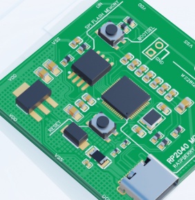
PCB design mainly needs to pay attention to the following aspects:
1. Manufacturing process requirements, manufacturing capabilities of board factories, and manufacturability design of PCB boards
2. Layout and wiring of power supply
3. Transmission line design
4. EMC
5. Clock design
Simply speaking, PCB design is to connect various devices so that the devices can work normally without affecting each other to complete the corresponding functions without interfering with each other. It is the basis of the entire product and determines the manufacturability and operation stability of the product. At the early stage of PCB design, it is necessary to pay attention to devise layout, stack planning, power supply division and so on. When wiring, you need to pay attention to the trace width of the high-speed signal and the distance from the reference ground. Беспроводной модем
This article aims to throw bricks and start jade, and briefly discuss some problems that may be encountered in the PCB design process. Because of the progress of production technology and the higher and higher signal rates, many things are only applicable to the present.
In terms of manufacturability, it can be seen from the aspects of PCB board production, component mounting, and subsequent maintenance.
The most common problems encountered in PCB production are how many layers of boards to use, how much line width, how much spacing, how big are the vias, and how much is the thickness of the board, from the simplest single-sided, double-sided, four-layer boards to the latter 20-layer boards , Generally, in order to control the cost, double-sided and four-layer are used. The double-sided side is that the front and back sides of the PP sheet are covered with copper skin, and the surface layer is sprayed with solder resist ink.
Generally, the two-layer boards are made of green ink. One is to protect the eyes: production and maintenance personnel need to stare at the PCB board for a long time. Compared with other colors, green ink is less irritating to the eyes and is not easy to fatigue. Green ink, PCB manufacturers use more green ink, the cost of green ink is lower than other ink procurement costs; at the same time, green ink is more obvious than black ink, and it is more convenient for staff to repair. For simple low-speed boards, two-layer boards are the most economical and suitable choice. Correspondingly, for complex high-speed boards, it generally starts with a four-layer board.
The four-layer board is the minimum number of board layers that can do impedance. (Generally, single-layer board factories just leave one layer empty in the multi-layer board.) High-speed PCBs need to pay attention to the impedance control of signal lines. Failure to do impedance matching for high-speed signal lines may cause signal reflection, loss, deformation, etc., resulting in circuit failure. The performance is not ideal or even the required functions cannot be realized. In high-speed PCB wiring, the trace impedance of digital signals is generally designed to be 50 ohms, which is an approximate figure. Generally, the coaxial cable baseband is 50 ohms.
Factors affecting the impedance of PCB traces mainly include the width of copper wire, the thickness of copper wire, the dielectric constant of the medium, the thickness of the medium, the thickness of the pad, the path of the ground wire, and the traces around the trace.
Because each factory has different material parameters, line compensation and potions for etching and plating. It is more reliable to assign the impedance to the PCB manufacturer. We only need to understand that the board thickness and line width and line spacing will affect the impedance, so we should be aware of it when designing. WIFI последовательный сервер
The smaller the via hole, the smaller the parasitic capacitance, and the smaller the space occupied on the board, but at the same time, the smaller the via hole, the higher the processing technology requirements, which increases the processing cost. On the other hand, the smaller the via hole, the more it can The current carried is also smaller. When designing a power supply, multiple large vias are often used to increase its overcurrent capability. Generally, double-sided panels use 0.3mm (inner diameter)/0.5mm (outer diameter) vias, four-layer The plate adopts 0.2mm (inner diameter)/0.3mm (outer diameter).
There is a certain relationship between the line width and spacing of PCB and the thickness of copper laying. Our boards generally use 1OZ, and only consider 2OZ when excessive current is required, or open the window and tin to increase the overcurrent capacity. The line width spacing of double-sided boards when copper is 1OZ is 0.127/0.127mm (5mil/5mil), multi-layer boards: 0.09/0.09mm (3.5mil/3.5mil), and the line width of double-sided and multi-layer boards when copper is 2OZ Spacing 0.2/0.2mm (8mil/8mil).
The PCB manufacturing process is not static. With the upgrading of board factory technology and the increase of signal rate, the current applicable rules may become inapplicable in the future. As a qualified engineer, you need to keep learning and understand the direction of cutting-edge technology in order to keep pace with the times. Enter.
PCB Design Considerations

6 min read
07 December 2022
In case you have found a mistake in the text, please send a message to the author by selecting the mistake and pressing Ctrl-Enter.
Беспроводной последовательный модуль lora 17
Ebyte — национальное высокотехнологичное предприятие, специализирующееся на исследованиях и разработках беспроводных модулей и промышленных IoT-терминалов. Неза...

No comments yet