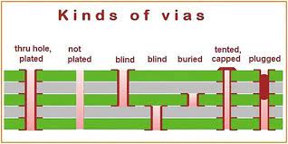
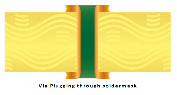
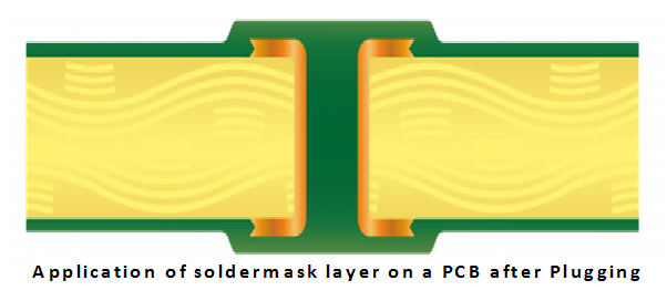
Via plugging entails the comprehensive infusion of resin or the application of a solder mask to fully enclose a via. This diverges from via masking, wherein the resin or solder mask offers mere coverage without filling the via.
The principal motivation behind via plugging is to forestall unintended solder flow within vias during the assembly or soldering phases. When not adequately sealed or obstructed, vias can permit solder to traverse downward from the pad, potentially engendering undesired solder connections.
The process of via plugging accommodates the use of either conductive or non-conductive materials. Vias imbued with conductive filler material prove instrumental in facilitating substantial current transmission from one facet of the PCB to another. Nonetheless, a notable drawback associated with conductive-filled vias centers on the incongruity in Coefficient of Thermal Expansion (CTE) between the conductive fill and the surrounding laminate. In the course of PCB operation, the conductive material's propensity to heat and expand at an accelerated pace compared to the adjacent laminate may precipitate fractures between the via walls and corresponding contact pads.
Vias replete with non-conductive material preserve standard via functionality. However, their capacity to bear elevated current loads akin to their conductive counterparts is constrained.
Deciphering the nuances of via plugging assists in making informed decisions on the type of via filling, aligning with the specific demands of the PCB design and application.

No comments yet